Block: hero
What Role Does Advanced Packaging Play in the Semiconductor Industry?
Powering high-performance computing and electronics for high-stakes environments.
Block: two_column
Semiconductor advanced packaging plays a crucial role in creating electronic devices that meet the power, performance, and functionality needs of demanding environments. These environments, ranging from defense and aerospace to AI-driven communications and automotive systems, require microelectronics that are not only smaller and faster but also thermally efficient and secure.
Advanced packaging enables heterogeneous integration of semiconductor materials, miniaturization, and increased interconnect density, making it a key differentiator for U.S. chip manufacturers. At the Florida Semiconductor Engine, we’re accelerating this shift by providing industry access to partners, skilled workforce pipelines, and a statewide ecosystem that unites our industry, educational institutions, government, and community research and commercialization.
Consider the autonomous vehicles used in defense missions, the AI capabilities embedded in smartphones, and the 5G networks powering global communication. All these applications depend on high-performance semiconductors made possible through advanced packaging. As demand grows for faster, smaller, and more efficient systems, the semiconductor industry is advancing packaging technologies that enable breakthroughs in computing power, energy efficiency, and system-level integration.

Block: centered_content
How Is the U.S. Responding to Offshore Dependence?
Today, 98% of advanced packaging is done off-shore, primarily in Asia, opening the door to malware and ill-intended players in the global realm. Reshoring this capability strengthens American security and prosperity, one of the Engine’s top priorities.
While global labor and supply chain economics have long influenced offshore adoption, the industry is responding with advanced automation, regionalized production strategies, and secure, trusted facilities. These efforts align with national priorities under the CHIPS Act and DoD-backed programs such as Microelectronics Commons, RESHAPE and SHIP, positioning the U.S., and Florida specifically, as a future leader in secure packaging capabilities. Companies looking to lead in this transformation can Join the Engine to access collaborative infrastructure, commercialization pathways, and a trusted semiconductor network.
Block: packaging_section
What Are the Key Technologies Behind Advanced Packaging?
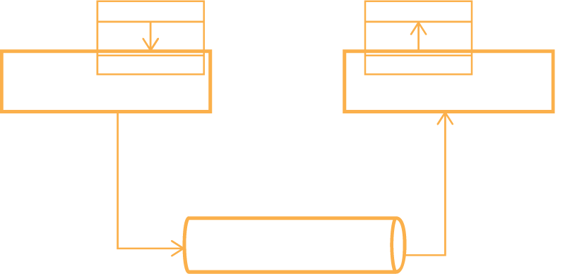
Advanced Packaging is the process of integrating disparate semiconductor materials, thermal solutions and multiple components in a high density electronic device in a way that maximizes performance and efficiency. Different technologies and techniques are used to combine an array of chips into smaller and smaller spaces. Advanced packaging technologies, such as wafer-to-wafer bonding, high density interposers and substrates, fan-out wafer-level packaging (FOWLP), and panel-level packaging, allow for the integration of multiple smaller chips manufactured from a multitude of materials into a single, high density electronic package, improving energy efficiency and computing power. These advanced packaging solutions are essential for supporting high performance computing (HPC), next-generation data centers, and complex applications in the automotive and defense sectors.
Heterogeneous Integration (HI) combines separately manufactured components and chips, often with distinct functions, into a single, 3-D, higher-level assembly. These advanced packages enable more versatile, efficient, and secure systems than traditional, 2-D packaging architectures. System-in-Package (SiP) architectures, for instance, integrate multiple dies to support sophisticated functionality, reduce latency, and drive performance in mission-critical environments.
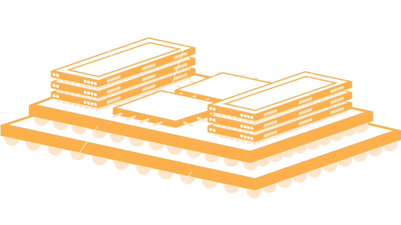
Integrating multiple chips into a single package condenses the space required for complex systems, enabling miniaturization. Electronic devices can get smaller and more compact without sacrificing computational power or functionality, a critical advantage for mobile platforms, embedded automotive computing, and AI. Advanced packaging techniques such as FOWLP and chiplet-based architectures are central to achieving these efficiencies.

Tighter integration of components leads to enhanced electronic performance. Data transfers up to 35 times faster with reduced lag, and closer component proximity lowers power usage and thermal output. This enables systems to operate reliably in demanding conditions. Innovations such as through-silicon vias (TSVs), interposers, and high-density redistribution layers (RDLs) ensure signal integrity and connectivity between logic, memory, and sensor components, pivotal in applications like autonomous systems and edge AI. Advanced packages and components also optimize thermal and power management in dense systems. Integrated device manufacturers (IDMs) and outsourced semiconductor assembly and test (OSAT) providers are investing in new design approaches to support high-volume, cost-effective manufacturing. Techniques like 2.5-D and 3-D integration are extending Moore’s Law by increasing transistor density and enabling parallel processing. The rise of machine learning, high-bandwidth memory, and massive-scale digital twinning model training (e.g., large language models) is accelerating demand for next-generation packaging solutions. Mechanical engineering plays a key role in the physical design of these components, especially in sensor fusion, MEMS integration, and structural reliability. With printed circuit boards (PCBs) acting as the bridge between advanced packages and larger systems, packaging has become the linchpin in enabling not just single-chip devices, but fully integrated, high-performance electronic systems.
Block: divider
Which Industries Benefit from Advanced Packaging?
Block: cards

Defense
Domestic packaging prevents tampering, reverse engineering, and cyberattacks on mission-critical electronic systems and devices.

Aerospace
Lightweight, reliable, compact electronics power communication and navigation systems to operate in the harsh environment of space.

Automotive Electronics
All vehicles and their electronic systems need semiconductors strong enough to survive high heat and intensity.
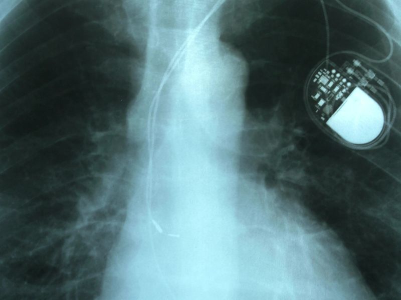
Medical
For wearable sensors, pacemakers, and other patient monitoring devices, faster data transmission is a life-or-death matter.
Block: flexible_columns
Expand Here
Does your business need access to skilled people, expansive space, and a strong ecosystem of support resources? You’ll find it in Florida.
Block: current_projects
Frequently Asked Questions
What is advanced packaging in semiconductors?
Advanced packaging refers to the integration of multiple chips or components into a single, high-density structure to improve system performance, reduce energy use, and enable miniaturization. It’s a foundational shift in how semiconductors are assembled and it’s reshaping the future of microelectronics.
How is advanced packaging different from traditional chip design?
Unlike traditional packaging, which often houses a single chip on a printed circuit board, advanced packaging brings multiple functions, logic, memory, sensors, into a tightly connected 3-D package. This supports faster data transfer, lower heat, and smarter integration across complex systems.
Why does advanced packaging matter for U.S. semiconductor production?
As 98% of advanced packaging is still done overseas, reshoring this capability is critical for national security, economic resilience, and global competitiveness. It enables the U.S. and Florida specifically to lead in trusted microelectronics for defense, AI, and next-gen communications.
What technologies are used in advanced packaging?
Techniques like wafer-to-wafer bonding, fan-out wafer-level packaging (FOWLP), system-in-package (SiP), and heterogeneous integration (HI) allow manufacturers to combine multiple dies in a single assembly. These methods unlock new levels of performance and design flexibility.
Who benefits from advanced packaging?
Industries with zero-fail expectations, defense, aerospace, automotive, AI, and medical, rely on advanced packaging to deliver reliable, secure, high-speed electronics in ever smaller spaces. It’s also critical for enabling future innovations in quantum, photonics, and edge computing.